Feature #5074
closedrestring of THT headers is rather small
Added by laforge about 3 years ago. Updated about 3 years ago.
100%
Description
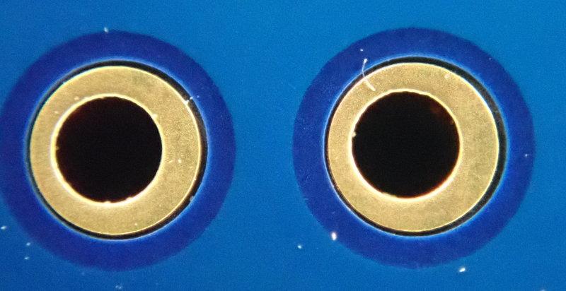
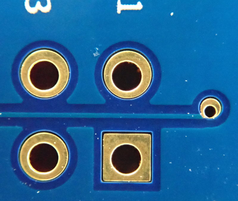
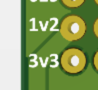
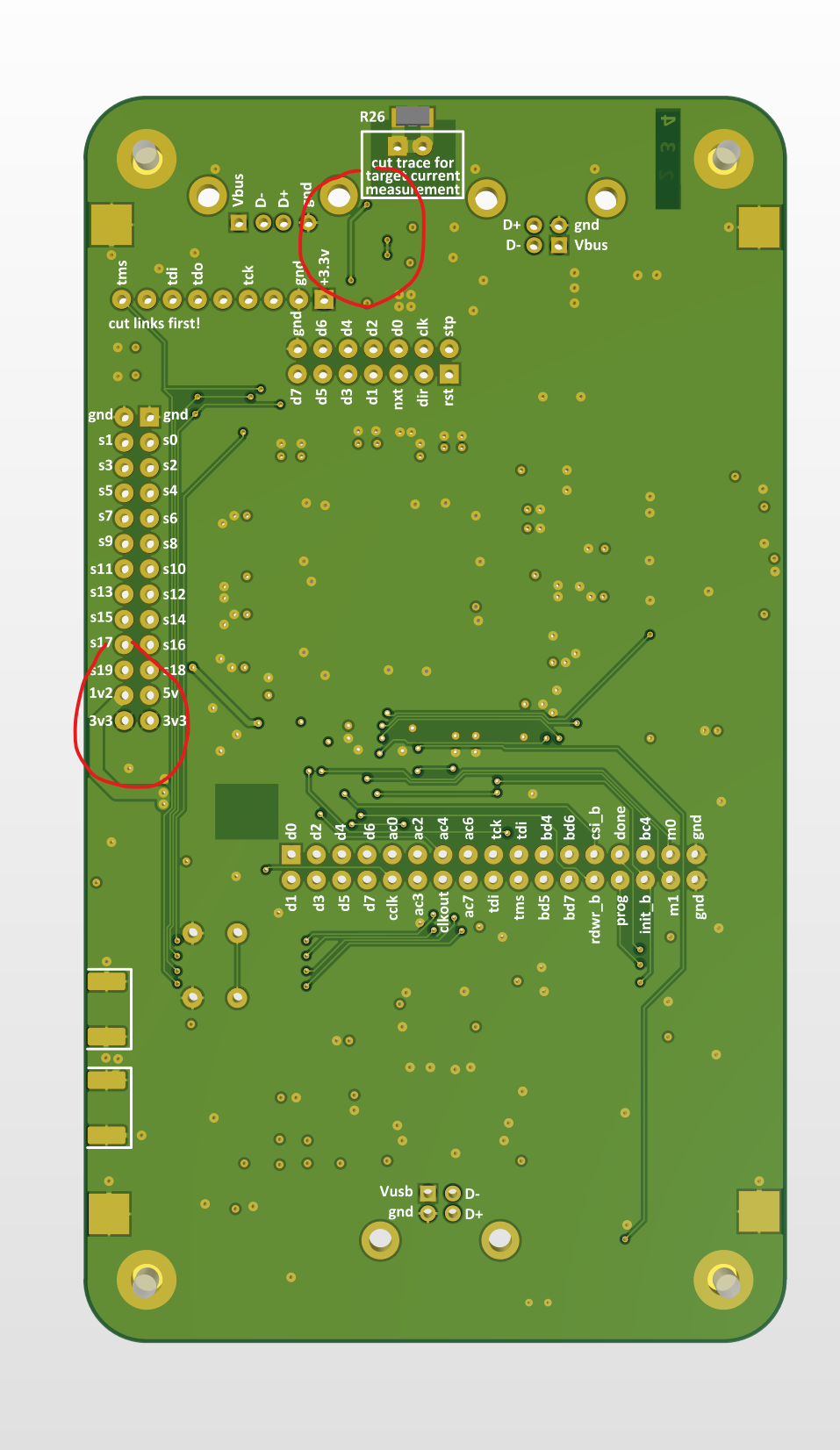
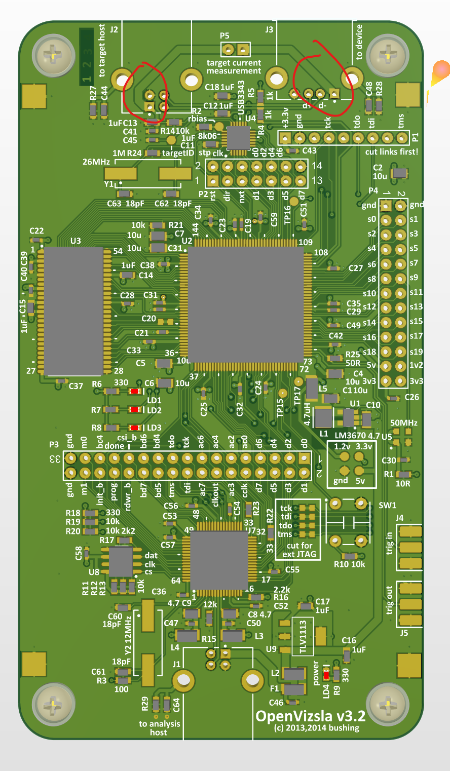
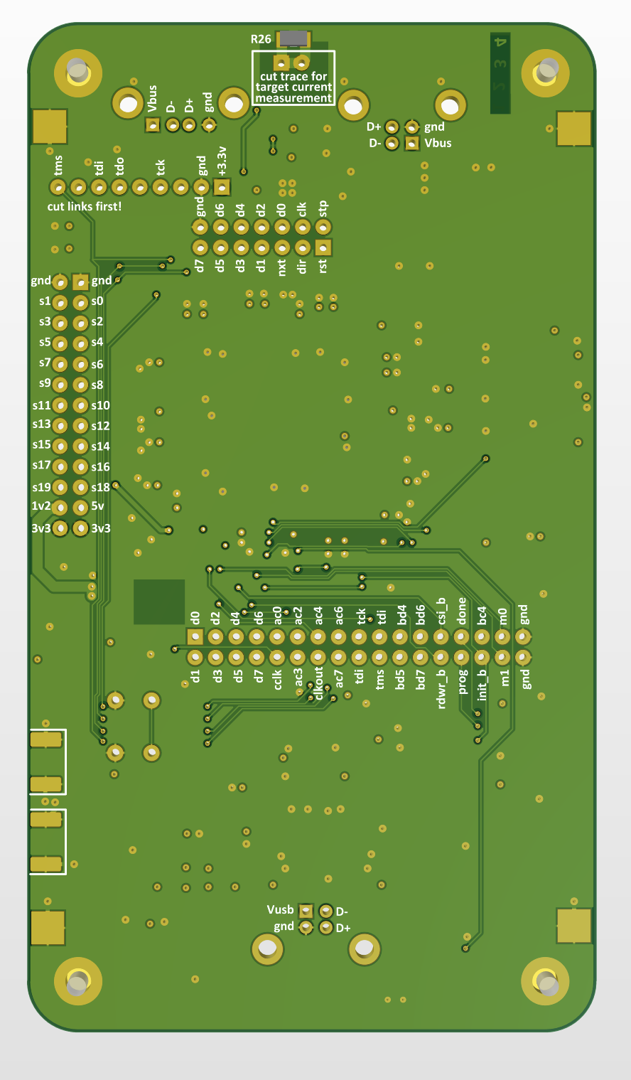
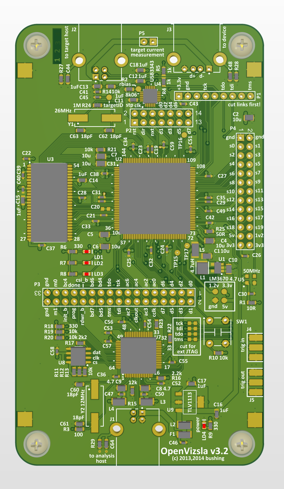
We don't populate the various 2.54mm pitch THT headers. However, in case users want to solder them to the board, I would think a larger "restring" would help solderability. The current one is rather small/thin. Not sure what our default in other designs is, mschramm?
Files
restring-THT-header2.jpg | View restring-THT-header2.jpg | 61.4 KB | mschramm, 03/15/2021 04:22 PM | ||
restring-THT-header1.jpg | View restring-THT-header1.jpg | 81.6 KB | mschramm, 03/15/2021 04:22 PM | ||
.5 annular ring.png | View .5 annular ring.png | 349 KB | cibomahto, 03/15/2021 05:04 PM | ||
annular-ring-05detail.png | View annular-ring-05detail.png | 67 KB | mschramm, 03/15/2021 08:24 PM | ||
before-back.png | View before-back.png | 363 KB | cibomahto, 03/15/2021 09:19 PM | ||
before-top.png | View before-top.png | 564 KB | cibomahto, 03/15/2021 09:19 PM | ||
after-back.png | View after-back.png | 336 KB | cibomahto, 03/15/2021 09:19 PM | ||
after-top.png | View after-top.png | 594 KB | cibomahto, 03/15/2021 09:19 PM |
Updated by mschramm about 3 years ago
- File restring-THT-header2.jpg restring-THT-header2.jpg added
- File restring-THT-header1.jpg restring-THT-header1.jpg added
- Category set to electronics
Those THT header's drill diameter is 0,9mm, for them a relaxed DRC would accept restrings not smaller than 0,254mm. In the current OV design they are 0,3mm, however, if they get drilled off-center (like on mine OV, see images), they end up being smaller than needed. The switch SW1 has drills of 1mm and a restring of 0,5mm which generally leaves more freedom when soldered by hand. So 0,5mm also for the pin header would be nice if no other clearance issues arise from this: the shown wire trace in the middle of the double-row header could be moved away, but on the top side of e.g. header P4 maintaining clearance might be more work.
Alternativly, IIRC, Altium allows to define different annular ring sizes for top-mid-bottom layers, so maybe for the bottom layer, a 0,5mm setting would be nice, where for the top (as well as for the inner) layer the 0,3mm setting could remain.
Updated by cibomahto about 3 years ago
- File .5 annular ring.png .5 annular ring.png added
You're correct that it's possible to change the pad sizes on a per-layer basis. Increasing just the bottom pad size to have a .5mm annular ring requires no layout changes, so it's a quick solution.
Updated by cibomahto about 3 years ago
- Status changed from New to In Progress
Updated by mschramm about 3 years ago
OK, nice - but please ease the situation with that power wire shown there like you solved it with VBUS elsewhere.
Updated by cibomahto about 3 years ago
Sure, I'll move it. Is it possible to state this in a more concrete fashion, so I can make a DRC rule? Something like a minimum spacing between power-class nets and thru-hole pads? I'm assuming the goal here is to decrease the chance of an assembly error during hand soldering. It's not totally clear to me the difference between this situation and the many smaller (data) traces that are routed through the pads on that connector.
For reference, the standard clearance on the board is 6 mils.
Updated by cibomahto about 3 years ago
- File before-back.png before-back.png added
- File before-top.png before-top.png added
- File after-back.png after-back.png added
- File after-top.png after-top.png added
Hopefully improved here: https://github.com/openvizsla/ov_ftdi/pull/46/commits/79dc1ebf1482506938d3722ed482db7fb99cddec
Updated by mschramm about 3 years ago
- Status changed from In Progress to Resolved
- % Done changed from 0 to 100