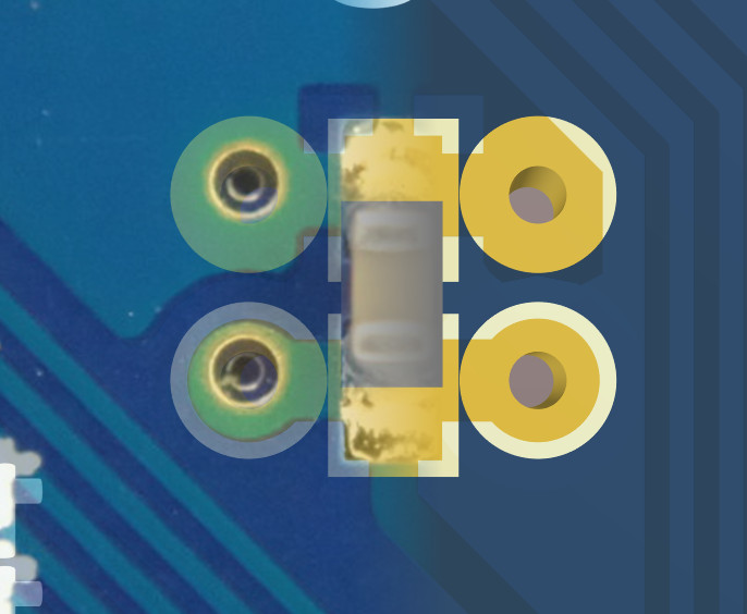
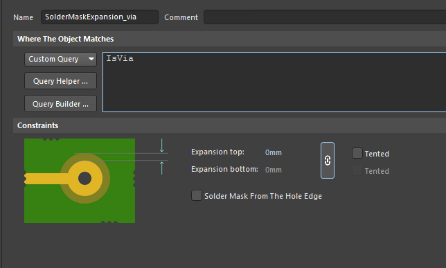
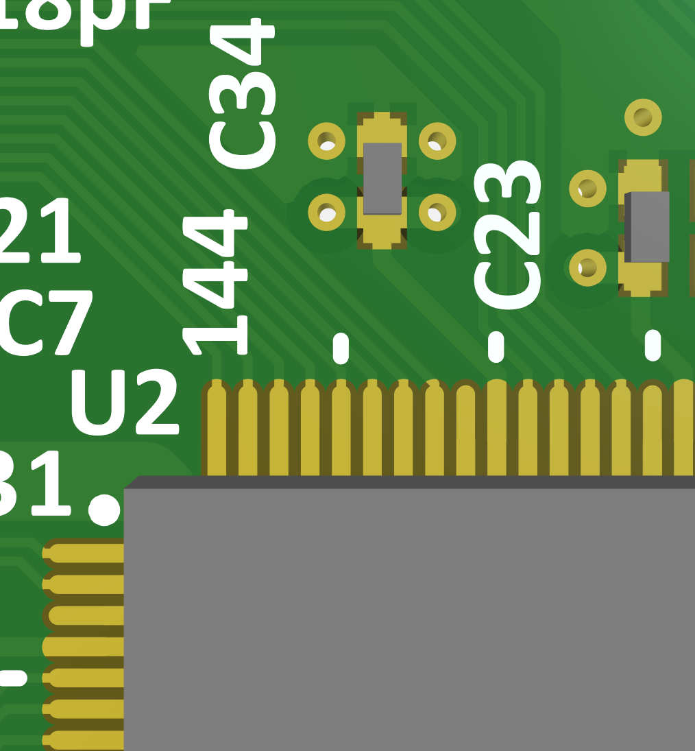
It took me a while to understand why this is the case in your project: your drills are twice the size of the ones in the produced PCBAs, so their restring fits almost into the size of your via drills: your vias are specified as 0,356mm, so the PCB house selects a tool diameter of 0,45mm. Together with your restring of 0,2mm it leads to a via diameter of 0,762mm and a solder mask opening (for untented vias) of 0,965mm - which is too big here. - The composed image lacks of projection equilization (plus off-center drills), but almost shows this as described.
Should I move the vias away from the components to avoid this?
No.
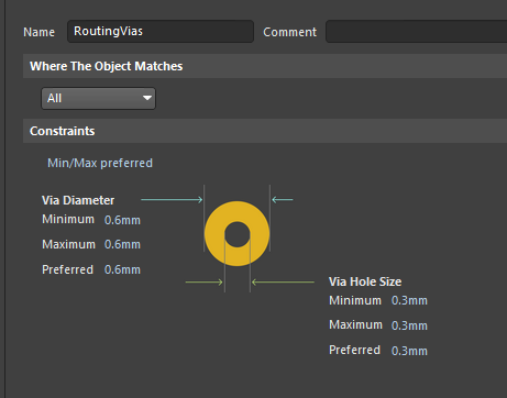
Generally please set all via size to 0,3mm, then the used tool will become 0,35mm (end diameter will become something like 0,25mm). Use a restring of 0,15mm - then all should fall into place. The board house takes care to a sufficient soldermask opening, so for the vias you could come (but don't need to) as close as 0,03mm with the SM to the via restring copper - it will get expanded anyway to the minimum if the SM lays on the copper.
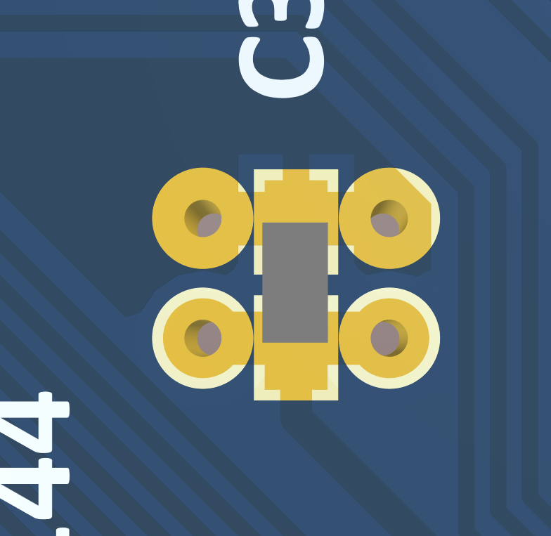
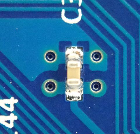
the motivation for exposing the vias
... is not only 'free test pads', but mainly the fact that for direct imaging the used thin ink for coating would require an additional via filling process with resin beforehand - which we clearly want to avoid.
What have been the respective values for these in the original file as they look even much smaller (like via 0,2mm + tool dia 0,25mm) ? Just curious.
.png)

