Bug #5108
closedadapt differential traces' properties to intended layer built-up for upcoming production run
Description
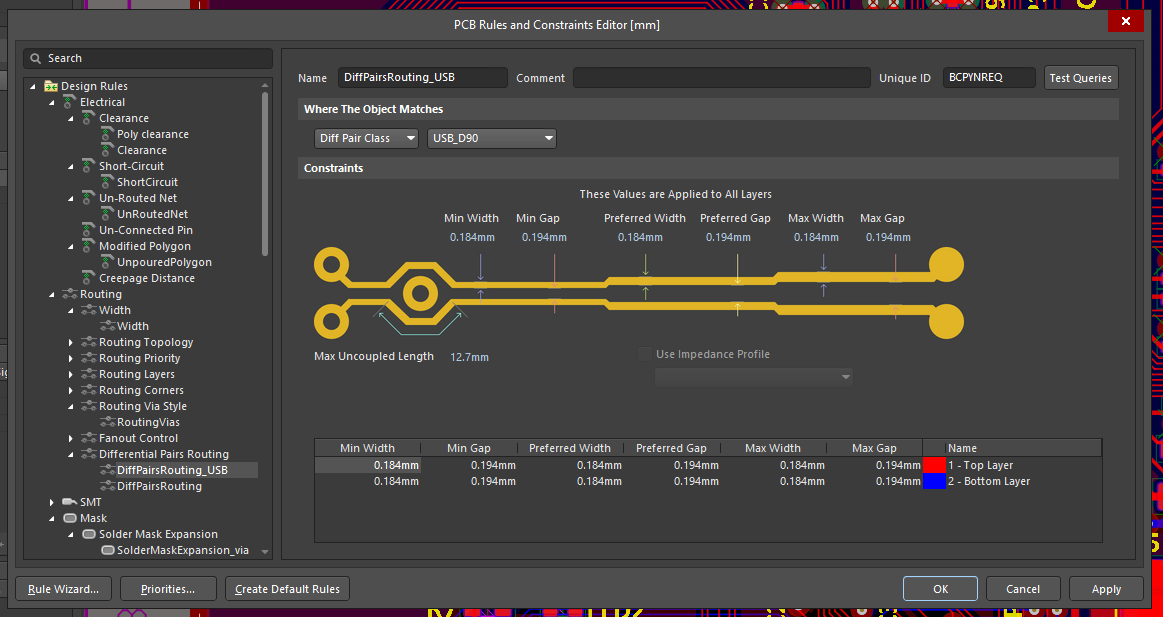
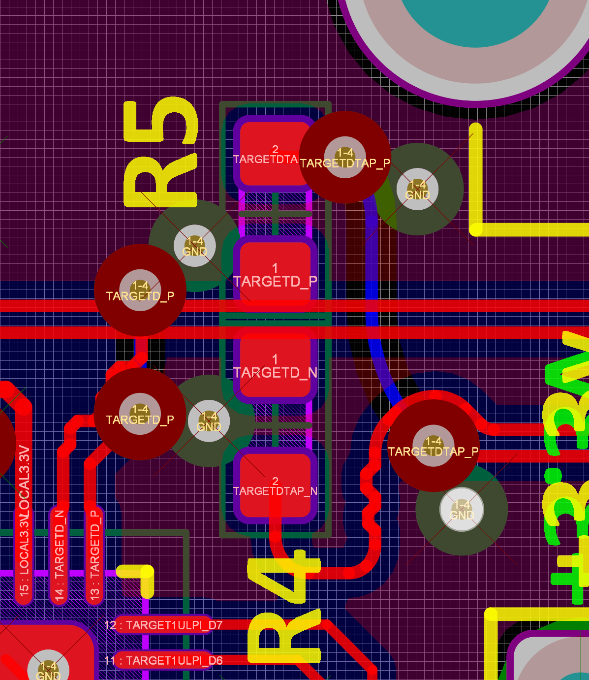
The layer stack-up of the orginal PCBAs differs to what we are going to produce. Changing the materials for the layer stack means no pooling option, so let's change the three differential pairs to the following values:
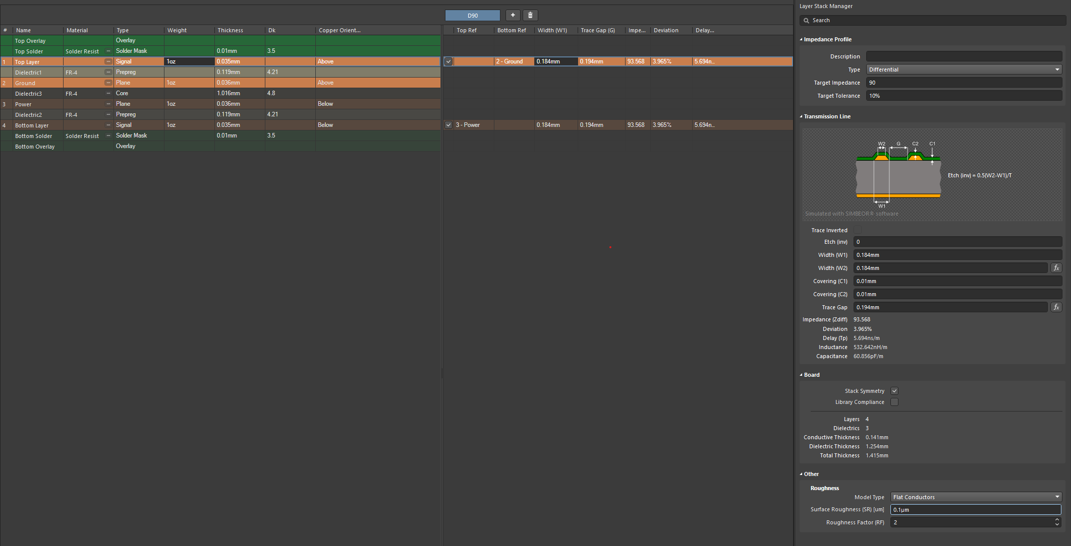
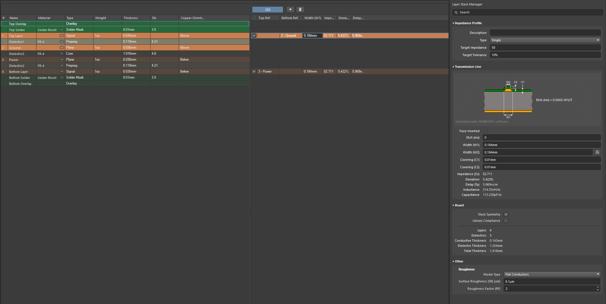
- wire track width: 0,184 mm
- wire track spacing 0,194 mm
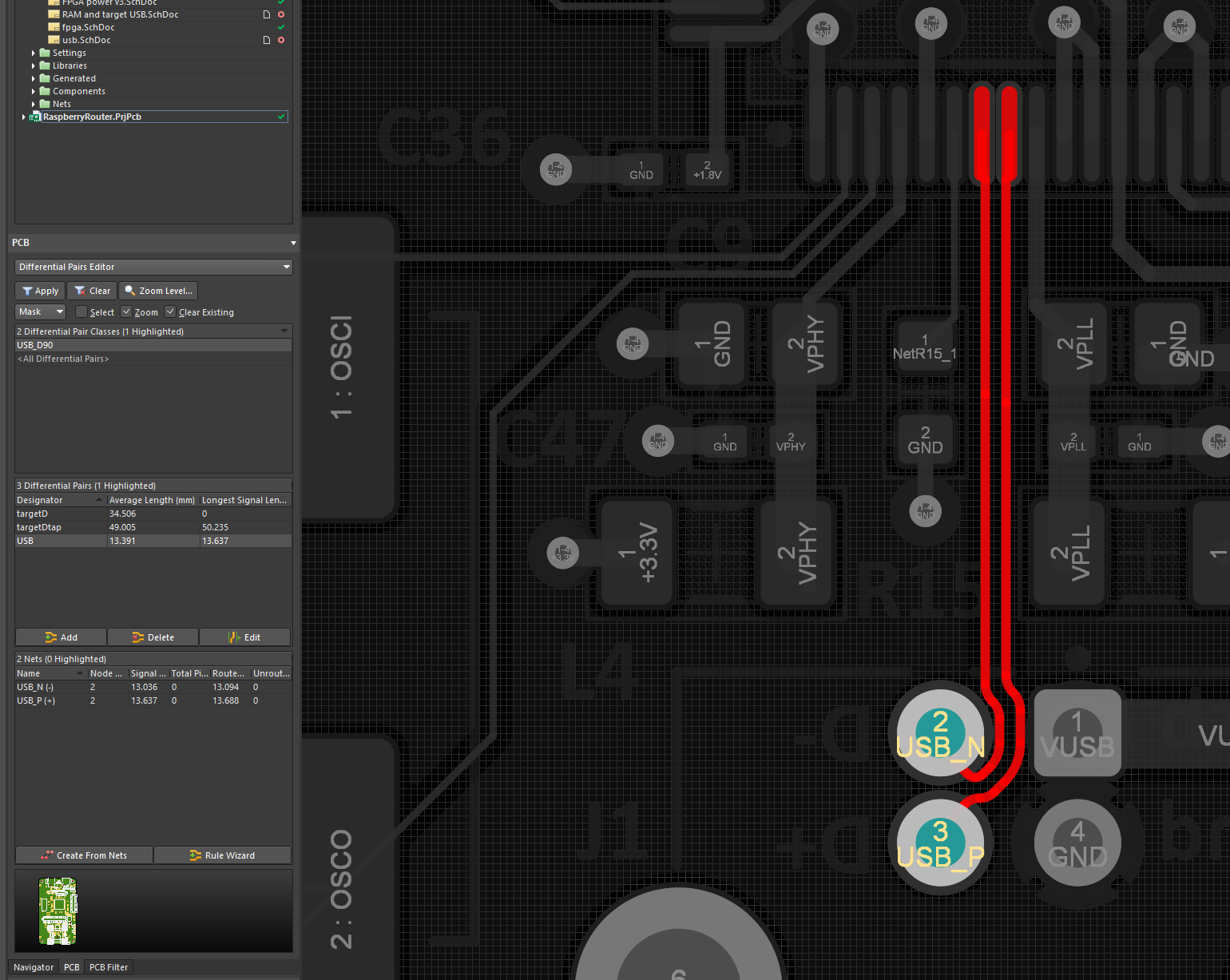
These values here result in characteristic impedance of 50 Ohms and a minimum differential impedance of 90 Ohms. Affected are the pairs
- TARGETDTAP_N / ~_P
- USB_N / ~_P
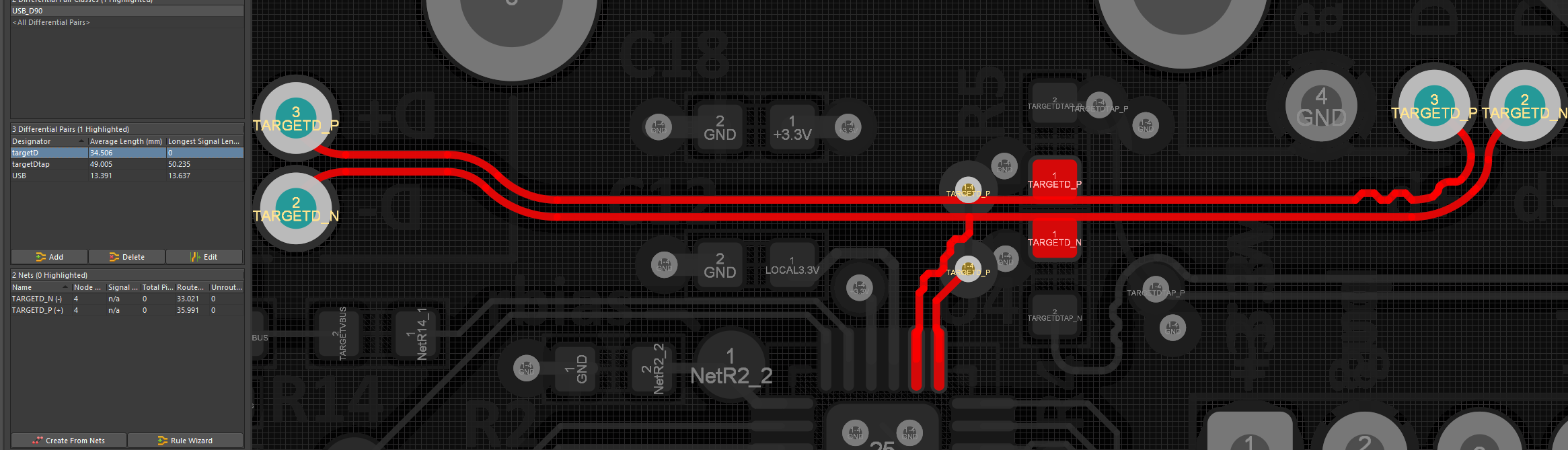
- TARGETD_N / ~_P
As discussed, please also make them a 'differential pair class'. We don't insist in sharp 45° angles, you might better want to go with bent traces.
The good news is that if the current design works with somewhat unmatched trace lengths and a nice T intersection, it should mean this is less critical than I might have imagined.
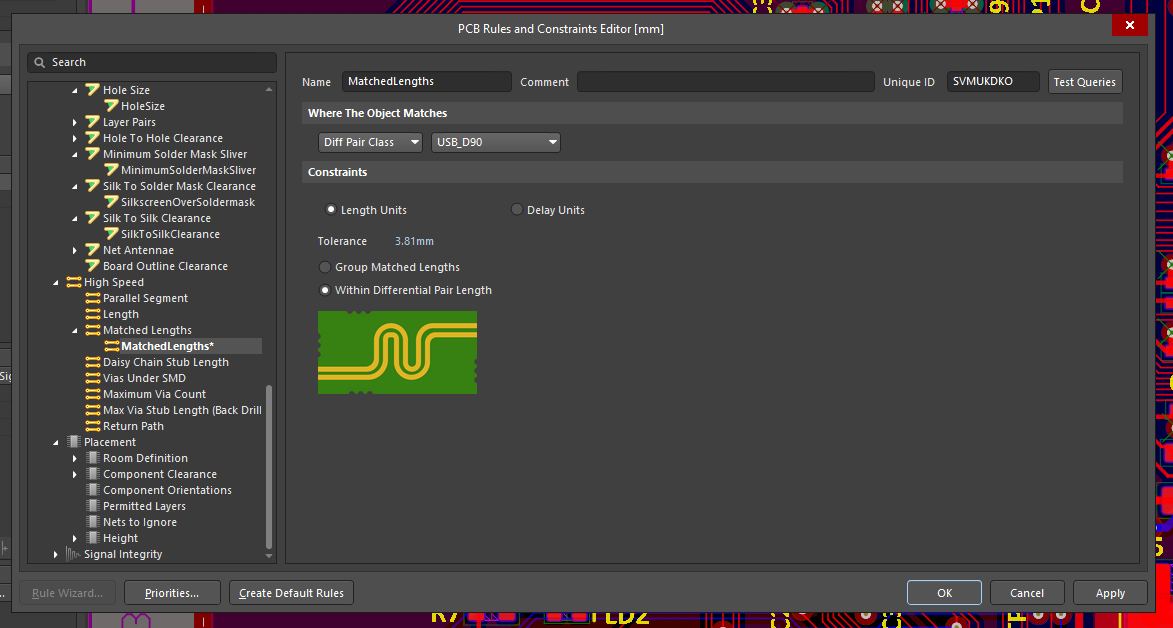
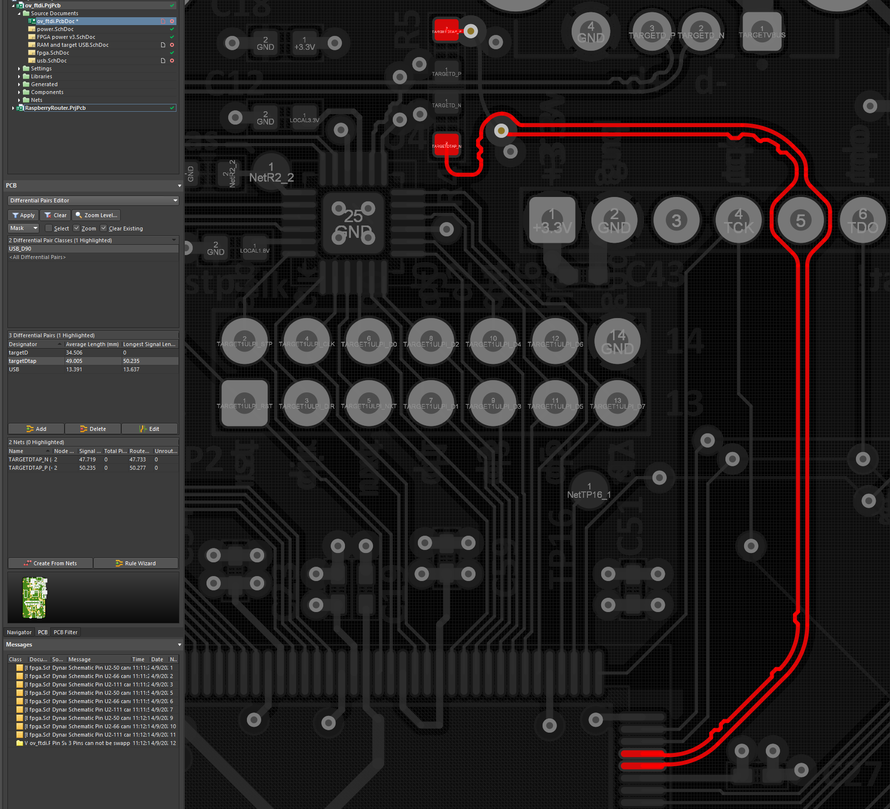
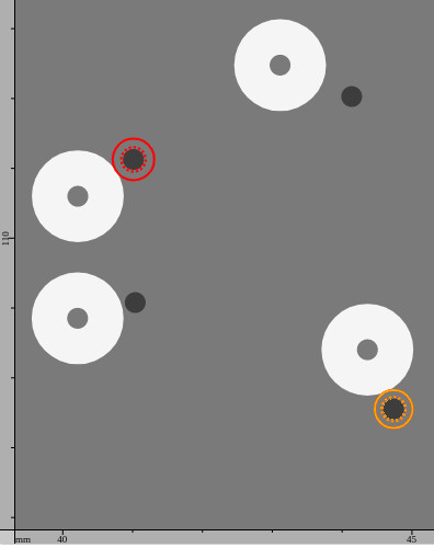
OK, but now we (you) can make it better! ;) Maintain a maximum pair lenght difference of less than 3,81mm (150mil), do a meander where the parallels are disturbed anyway, and not at a sane end. This might only be needed for TARGETDTAP_*, which unfortunately crosses a THT header. Don't introduce more vias on those traces.
If you want to 'play' with the inbuilt diff pair helper tool (or another tool of your choice): at 500 MHz, the material has an Er= 4,21. Layer distance (height of dielectricum) is 0,119mm, end copper is 35µm. And let me hear your results, if the Altium helper tool is far off the mentioned values.
Files