Bug #5066
closedconnect mounting holes to GND plane
100%
Description
The four mounting holes are plated, but not connected to the GND layer. Let's change that.
Files
Updated by laforge about 3 years ago
- Assignee changed from mschramm to cibomahto
- Priority changed from Normal to Low
Updated by cibomahto about 3 years ago
- Status changed from In Progress to Resolved
Updated by cibomahto about 3 years ago
- Status changed from Resolved to In Progress
Updated by mschramm about 3 years ago
- % Done changed from 0 to 80
Do I see this right that the mounting holes are connected to GND via thermals only on the inner layers (more specific: on one inner layer), but not on top and botom copper? I'm fine with that, just curious.
Updated by cibomahto about 3 years ago
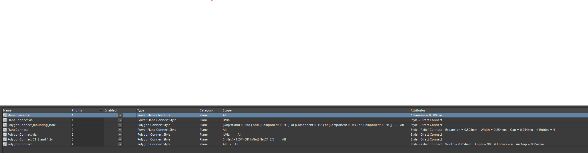
- File plane DRC rules.png plane DRC rules.png added
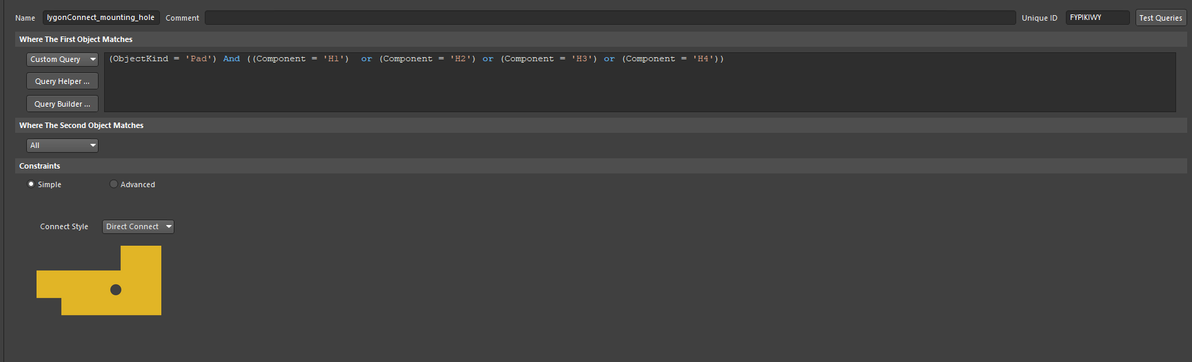
- File mounting_hole_to_polygon.png mounting_hole_to_polygon.png added
Good catch. Yes, that's true- I added a rule to connect the mounting holes to polygons without thermals ('direct connect' in Altium terminology), but forgot to add one for the inner (plane-style) layer. It's easy enough to leave it as-is, or change it.
This design was made with the inner layers specified as a 'plane' type in Altuim (which is why they are inverted in the Gerber outputs). This is fine, however it has the result of using separate design rules for the inner layers vs the outer layers.
For reference, I've included a snapshot of all the plane rules. The rules (in order of priority) are:
1. On the inner (plane) layers, clearance between non-connected vias and the plane are .508mm.
2. On the inner (plane) layers, vias that are connected to the plane are connected directly.
3. On the inner (plane) layers, non-via drills (thru-hole pads, for instance the mounting holes, and the ones in the .1" headers) are connected with a thermal relief ('relief connect' in Altium terminology). These have an expansion (restring) of .508mm, a .254mm conductor width, and a .254mm air gap.
4. On the top and bottom (polygon) layers, vias that are connected to a polygon are directly connected without thermals (effectively the same as the plane layers)
5. The four mounting holes specifically are connected directly, without thermals (I added this rule).
6. All other pads are connected to pads via a thermal; this has a .254mm conductor width, and a .254mm air gap. There is an a separate open issue ( https://osmocom.org/issues/5065 ) to modify this for at least some of the top-and-bottom layer pads.
Updated by mschramm about 3 years ago
- Status changed from In Progress to Resolved
- % Done changed from 80 to 100
also done! thx

