Bug #5065
closedthermals are too narrow
100%
Description
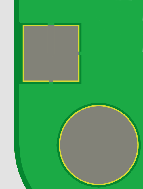
The "gaps" of the thermals around pads are too small for our taste. There should be wider copper and less "gap"
Files


Updated by cibomahto about 3 years ago
- File original 0.254mm gap, 0.254mm conductor.png original 0.254mm gap, 0.254mm conductor.png added
- File increased to 0.381mm gap, 0.508mm conductor.png increased to 0.381mm gap, 0.508mm conductor.png added
Should this apply to the small component pads as well? My concern would be that increasing the conductor width on the 0402 components might result in them being unbalanced thermally.
I see three options here:
1. Increase all thermal connects, say from the original 0.254mm gap/0.254mm conductor spec to 0.381mm gap/0.508mm conductor (as pictured)
2. Make a new rule, and only apply it to larger pads (such as the one in the example)
Updated by mschramm about 3 years ago
- Status changed from Feedback to In Progress
- Priority changed from Normal to Low
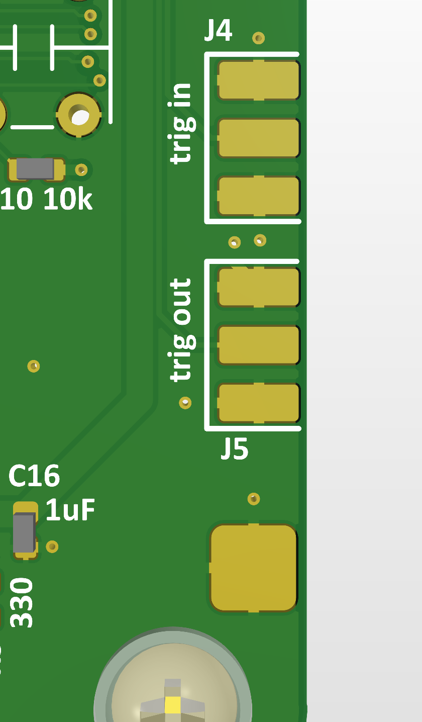
on another topic (#5066):
to modify this for at least some of the top-and-bottom layer pads
yes. I think we should minimize efforts here. - Thanks for your explanation in #5066. The thermals look good for traces like the ones you pictures in #5066#note-3 for parts like e.g. 0402. We can boil down our concerns to those ones like the four GND pads close to the mounting holes and especially the ones on the SMA footprints. Let's only change those ones mentioned, from 0,254mm trace width to 0,508mm (top and bott).
Updated by cibomahto about 3 years ago
- File after-bottom.png after-bottom.png added
- File after-top.png after-top.png added
- File design_rule.png design_rule.png added
Implemented here: https://github.com/openvizsla/ov_ftdi/pull/46/commits/0067bd55dc7637188a5d1bcd3c35602e1a6e9866
Rule added to change the thermals on just those footprints.
Updated by mschramm about 3 years ago
- Status changed from In Progress to Resolved
- % Done changed from 0 to 100
solved; thanks!

