Feature #5064
closedNo tented (covered with solder resist) vias
100%
Description
We don't want solder resist nor silk screen on top of the vias. Let's make sure they are always exposed.
Files
.png)
Updated by laforge about 3 years ago
- Subject changed from No tented (covered with silkscreen) vias to No tented (covered with solder resist) vias
Updated by laforge about 3 years ago
- Description updated (diff)
- Assignee deleted (
mschramm)
Updated by cibomahto about 3 years ago
- File untented vias.png untented vias.png added
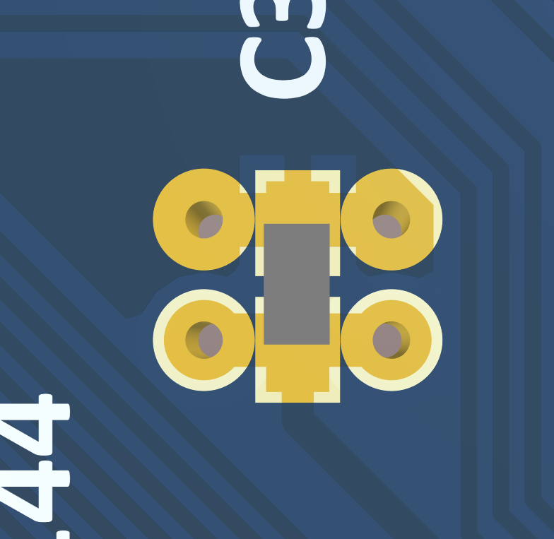
Un-tenting the top side vias creates some soldermask sliver issues, particularly with the bypass caps around the FPGA. Should I move the vias away from the components to avoid this? And in that case, is there a particular minimum soldermask sliver specification that should be followed?
Updated by cibomahto about 3 years ago
As an alternative, if the motivation for exposing the vias is to facilitate probing signal traces, it's possible to leave tenting on this sort of power via.
Updated by mschramm about 3 years ago
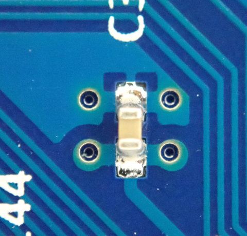
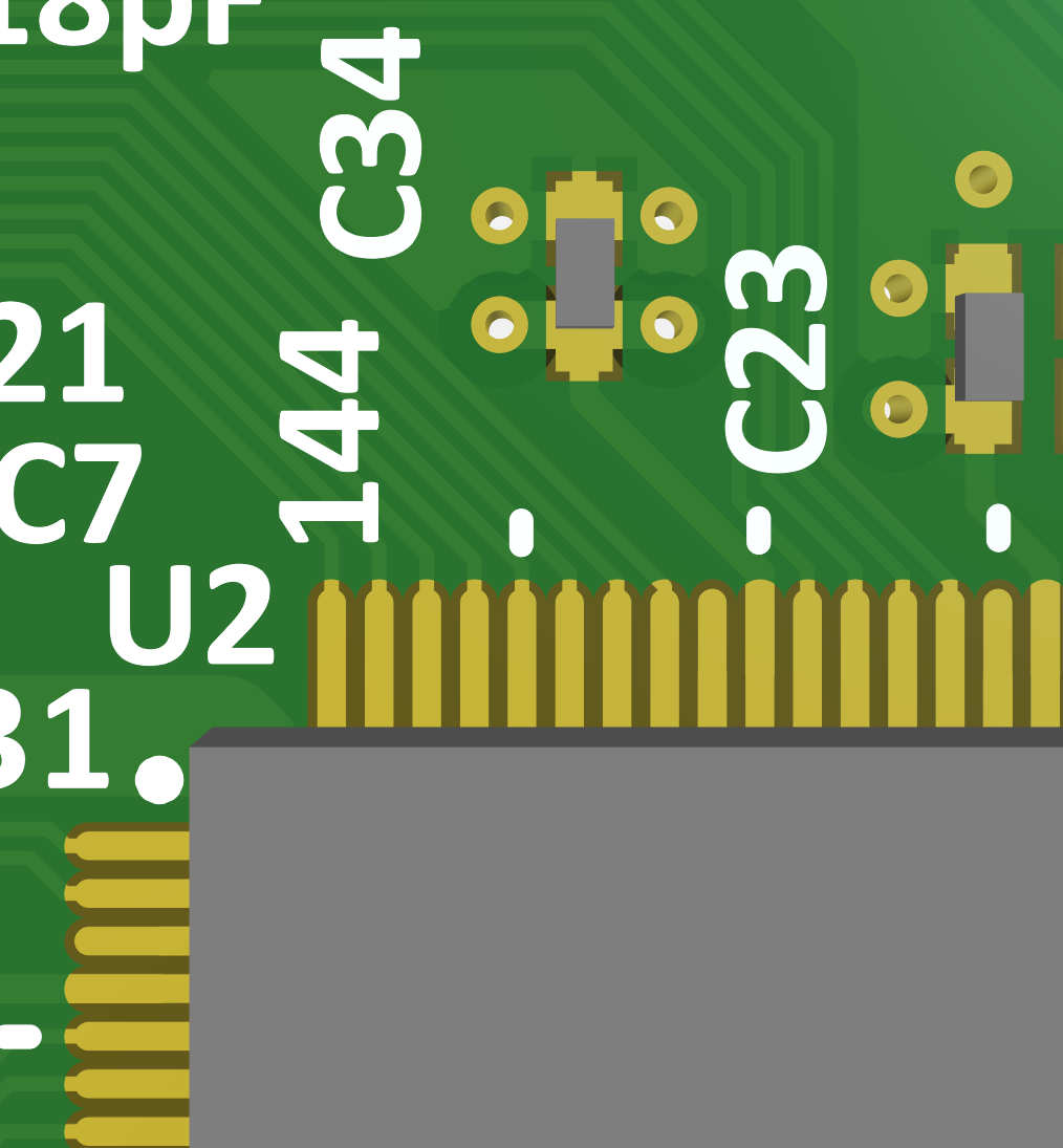
- File C34-vias.jpg C34-vias.jpg added
this is what it looks like in reality by now:
(I'll come up on Tue with a suggestion about it, maybe even a DRC file)
Updated by mschramm about 3 years ago
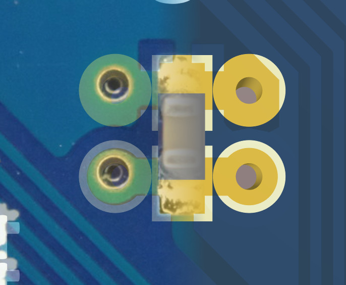
- File untented_vias-composite.jpg untented_vias-composite.jpg added
- Status changed from Feedback to In Progress
It took me a while to understand why this is the case in your project: your drills are twice the size of the ones in the produced PCBAs, so their restring fits almost into the size of your via drills: your vias are specified as 0,356mm, so the PCB house selects a tool diameter of 0,45mm. Together with your restring of 0,2mm it leads to a via diameter of 0,762mm and a solder mask opening (for untented vias) of 0,965mm - which is too big here. - The composed image lacks of projection equilization (plus off-center drills), but almost shows this as described.
Should I move the vias away from the components to avoid this?
No.
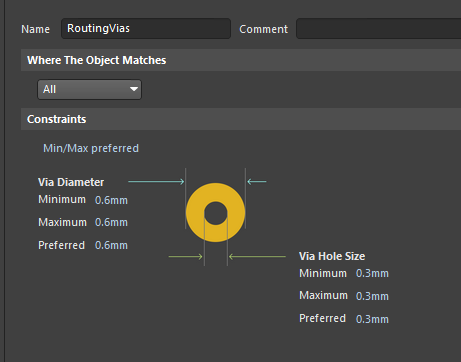
Generally please set all via size to 0,3mm, then the used tool will become 0,35mm (end diameter will become something like 0,25mm). Use a restring of 0,15mm - then all should fall into place. The board house takes care to a sufficient soldermask opening, so for the vias you could come (but don't need to) as close as 0,03mm with the SM to the via restring copper - it will get expanded anyway to the minimum if the SM lays on the copper.
the motivation for exposing the vias
... is not only 'free test pads', but mainly the fact that for direct imaging the used thin ink for coating would require an additional via filling process with resin beforehand - which we clearly want to avoid.
What have been the respective values for these in the original file as they look even much smaller (like via 0,2mm + tool dia 0,25mm) ? Just curious.
Updated by cibomahto about 3 years ago
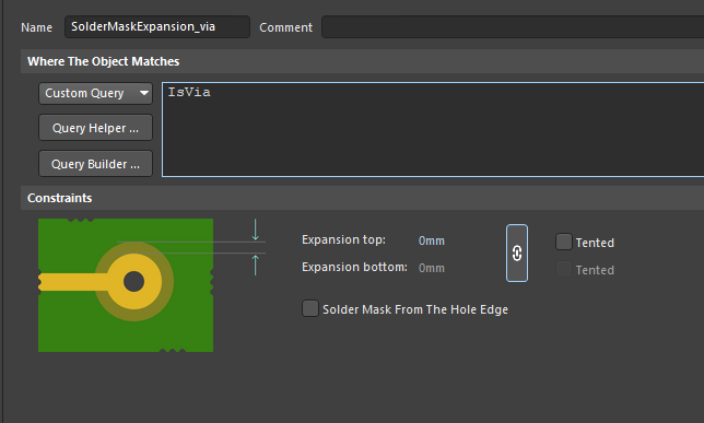
- File via rule.png via rule.png added
- File soldermask expansion for via.png soldermask expansion for via.png added
- File after.png after.png added
- File after(whole board).png after(whole board).png added
Implemented here: https://github.com/openvizsla/ov_ftdi/pull/46/commits/fb80441ae0aa444fdb9ee658fa87f5b66ef974c3
It took me a while to understand why this is the case in your project: your drills are twice the
size of the ones in the produced PCBAs, so their restring fits almost into the size of your via
drills: your vias are specified as 0,356mm, so the PCB house selects a tool diameter of 0,45mm.
Together with your restring of 0,2mm it leads to a via diameter of 0,762mm and a solder mask
opening (for untented vias) of 0,965mm - which is too big here. - The composed image lacks of
projection equilization (plus off-center drills), but almost shows this as described.
Yes, the design was inherited with the following via sizes:
.330mm drill: 4 vias (under U4)
.356mm drill: 239 vias, mixed between .61mm and .762mm diameter pad size
On the bottom side of the boards, the un-tented vias had a 4mil spacing between the edge of the copper pad and the soldermask (solder mask expansion in Altium terminology)
Ok, I:Generally please set all via size to 0,3mm, then the used tool will become 0,35mm (end diameter will
become something like 0,25mm). Use a restring of 0,15mm - then all should fall into place. The board
house takes care to a sufficient soldermask opening, so for the vias you could come (but don't need
to) as close as 0,03mm with the SM to the via restring copper - it will get expanded anyway to the
minimum if the SM lays on the copper.
- updated all vias to have .3mm drill / .6mm pad size -> .15mm restring (FWIW, Altium uses pad size as the driving dimension, not restring)
- Created a new DRC rule to enforce the .3mm/.6mm via geometry
- set all vias to be untented
- Created a new DRC rule to enforce a 0mm soldermask expansion on vias (so that the soldermask lines up directly with the outside of the via pad/restring area)
If you'd like the other soldermask openings around the SMD components to also have 0mm expansion, let's create a new issue for it. Note that the inherited design rule for soldermask expansion makes a .102mm gap from the outer edge of the pad copper to to the soldermask pad.
... is not only 'free test pads', but mainly the fact that for direct imaging the used thin ink
for coating would require an additional via filling process with resin beforehand - which we clearly want to avoid.
Interesting, thanks for the explanation.
Updated by mschramm about 3 years ago
Thanks, I immediately will check this by uploading it to the PCB house.
cibomahto wrote:
... is not only 'free test pads', but mainly the fact that for direct imaging the used thin ink
for coating would require an additional via filling process with resin beforehand - which we clearly want to avoid.Interesting, thanks for the explanation.
Note that this strongly depends on the technology used by the board house: if another manufacturer does not use direct imaging, laser plotters or thelike, or simply a different ink viscosity as their house rule, then the former will not apply.
Updated by mschramm about 3 years ago
- Status changed from In Progress to Resolved
- % Done changed from 0 to 100
verified; looks good to me and the PCB house, thanks!

